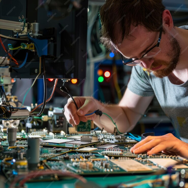
Forcyst is a leading provider of Electronics Manufacturing and Engineering Design Services with over eight years of experience. We specialize in offering end-to-end solutions in electronics manufacturing, encompassing everything from product design to testing. Our commitment to precision, quality, and innovation has earned us the trust of clients across various industries. By continuously focusing on research and development, Forcyst remains at the forefront of technological advancements in electronics.
Key Offerings

Electronics Manufacturing Services (EMS):
• Product Design
We collaborate closely with our clients to design innovative, efficient, and cutting-edge electronic solutions tailored to their needs.
• Materials Management & Supply Chain
From sourcing components to managing inventory, we ensure a seamless supply chain for smooth operations.
• Testing & Quality Assurance
Our rigorous testing procedures guarantee that all manufactured products meet the highest industry standards.
• Repair & Maintenance Services
We provide comprehensive post-production support, ensuring the longevity of products and enhanced customer satisfaction.

Engineering Design Services
• Product Development
Our team of skilled engineers transforms concepts into functional prototypes and final products.
• Prototyping
We develop functional prototypes for thorough testing and validation before production.
• Re-engineering
Forcyst optimizes existing designs to enhance performance and efficiency.

End-of-Life Planning
We assist OEMs with last-time buys of obsolete parts and redesign strategies to extend product life.

Innovation and Research & Development
Our commitment to precision and quality drives continuous innovation. We stay ahead of industry trends and technological advancements.
At Forcyst, our client-centric approach, technical expertise, and dedication to excellence solidify our position as a trusted partner in the electronics manufacturing industry.

What we do

PCB Designing

PCB Fabrication

PCB Assembly

PCB Stencil

Component Sourcing

Box Build Assembly

Turnkey Manufacturing Solutions
Our Capabilities

PCB Fabrication: 1 to 20 Layers PCB Manufacturing, Rigid & Flexible PCB Fabrication
• PCB Layers
1 to 20 Layers (Rigid), Single-sided, Double-sided (Flex)
• PCB Material
FR-4: Tg135/Tg140/Tg155/Tg170, Aluminum (1 W/m.K), Copper Core (380 W/m.K), Rogers/PTFE Teflon
• PCB Dimensions
5x5mm-400x500mm (Rigid), 20x20mm-230x470mm (Flex), Dimension Tolerance: ±0.1mm
• PCB Thickness
Board Thickness: 0.4-2.5mm, Thickness Tolerance: ±10% (Thickness ≥1.0mm), ±0.1mm (Thickness <1.0mm)
• Copper Layer Thickness
Outer Layer: 35µm / 70µm, Inner Layer: 17.5µm/35µm/70µm
• Surface Finish
HASL (Leaded, Lead-Free), ENIG (Flex & Rigid)
• Solder Mask
Color options: Green, Red, Yellow, Blue, White, and Black; Minimum Solder Bridge: 0.10mm
• PCB Penalization
Panel Spacing: ≥22.0mm, ≥20x20mm (Round Board), Breakaway Tab Minimum Width: 4mm, Edge Rails Minimum Width: 3mm
• Drill Hole Size
0.15-6.30mm, Tolerance: +0.13/-0.08mm, Minimum Via Hole Size: 0.15-0.25mm, Pad Size: ≥1.0mm, Hole Clearance: 0.5mm
• PCB Track
Minimum Track Width: 0.125mm (1-2 Layers), 0.09mm (4+ Layers), Minimum Track Spacing: 0.125mm (1-2 Layers), 0.09mm (4+ Layers)
• BGA Dimensions
Minimum BGA Pad Dimension: 0.25mm, Minimum BGA Pad Spacing: 0.125mm
• Miscellaneous Offerings
No MOQ, Castellated Holes, Edge Plating, 4-Wire Kelvin Test, Paper Between PCBs, Blind Vias, Peelable Solder Mask

PCB Assembly: Fully Automated SMT Line Wave Soldering for THT Components
• PCB Assembly Variant
Surface Mount (SMT), Through-Hole (THT), Mixed Technology (SMT / Through-Hole), Single or Double-sided Placement
• Types of Solder
Leaded and Lead-free (RoHS Compliant)
• Component Types
QFN & QFP: 0.2mm Pitch, BGA: 0.25mm Pitch, Passive Components: 0402, Small Chip Packages: 0201, Max Size: 50x50x10mm
• Component Packages
Reels, Cut Tape (Continuous and 300mm+ length), Tube, Tray (Max Panel Size: 200x300mm)
• PCB Dimensions
Min. Board Size: 50x50mm (Panel form for Smaller PCBs), Max. Board Size: 300x450mm, Acceptable Board Thickness: 0.5mm-2mm
• PCB Shape
Rectangular & Circular; Custom Shapes will require penalization (Leaded, Lead-Free), ENIG(Flex & Rigid)
• PCB Type
Rigid Flex (Manual Assembly Only)
• PCB Quality Control
ESD Protected Assembly, Clean Rooms, On-Line Quality Control, Aqueous PCB Cleaning
• Assembly Capacity
Manual Assembly: 50,000 Solder Points/Day, Machine Assembly: 300,000 Solder Points/Day, Machine Assembly: 3,00,000 Solder Points/Day
• Assembly Inspection
Visual Inspection, Microscope-Assisted Inspection, In-Circuit Testing
• Miscellaneous Offerings
No MOQ, No Setup Cost, Minimum Lead Time of 24 hours, Clean Rooms, 100% Traceability, 15-Day Repair Warranty

PCB Stencil: Framed / Frameless SMT Stencil Japanese Grade Fine- grain Sheets
• Stencil Material
Stainless Steel and Mylar
• Stencil Size
Stainless Steel Stencil: 18x18", 23x23", 29x29", 17x36", 23x36", 17x55", 17x58", 20x55", 20x58", 23x55", 23x58", Mylar Stencil: 18"x18"
• Stencil Thickness
Stainless Steel Stencil: 0.4mm, 0.5mm, 0.6mm. Mylar Stencil: 0.6mm.
• Polishing Process
Sanding, Etching, and Electropolishing.
• Manufacturing Accuracy
Minimum Aperture Accuracy: ±5µm. Positioning Accuracy: ±10µm.
• Miscellaneous Offerings
No MOQ, Minimum Lead Time of 3 Working Days, High-grade Material, Mirror Finish.
BOX BUILD ASSEMBLY:
- Electromechanical Assembly, Panel & Cabinet Wiring, Software Loading & Configuration, Enclosure Stickering and Printing, Product Packaging, Cable Harness Assembly, Conformal Coating Protection, Enclosure Fitting and Waterproofing, Product Serialization and Barcoding, Custom Tooling & Fixtures.
TURNKEY MANUFACTURING:
- Simplified Supply Chain Management, Quality Assurance, Easily Scalable, Focus on Core Competencies, Cost Efficiency, Reduced Risk, Centralized Expertise, Innovation, and Information Integrity.
